News
Clever concepts for exploiting energy
Energy permeates our lives—no natural process can function without it. We need energy to move, lift, heat, light and accelerate objects. And it’s also true that wherever energy is used, there are ways of capturing, generating and saving it. Indeed, many, possibly hundreds of solutions to this end have been developed—even aside from well-known technologies like solar panels, reservoirs and wind turbines.
One such solution is harnessing powerful ocean currents on coastlines: over half a century ago, one of the world’s largest tidal power plants was built on the shores of Brittany, in western France. While tidal power converts the energy difference between low and high tide into electricity, the related technology of wave energy exploits the motion of individual waves for power generation. Aside from a few exceptions, however, wave energy systems have yet to progress beyond the experimental phase.
But not only natural forces are sources of energy: human beings can also function as power generators. During their four-year world tour, British rock band Coldplay are aiming to convert human energy into electricity by using kinetic dance floors whose surface consists of modules, in the form of panels, that sink slightly when fans dance on them. Part of this movement is stored in the panels as energy, which can then be used to power things like lighting. As another way to tap into “people power”, researchers are creating special fibres for knitwear or T-shirts that enable the wearer to generate electricity just by moving.
Small changes, big difference
The conversion of kinetic energy into electricity is based on the principle of piezoelectricity: when mechanical pressure is applied to certain materials, it causes the existing electric charge points to shift in such a way that an electric voltage arises. Piezoelectricity is just one example of how energy can be generated on a small scale, and how processes can be made more energy efficient.
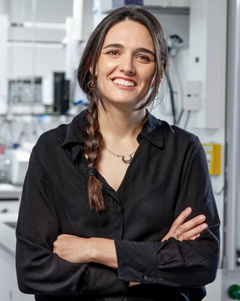
The key to success in this area often comes down to making incremental changes to a material that nonetheless bring about significant changes in its properties. Physicist Maria Ibáñez at the Institute of Science and Technology Austria (IST Austria) in Klosterneuburg near Vienna is specialised in one such approach: developing novel nanomaterials and investigating their properties. She says: “When we work on the nanoscale, we observe entirely new phenomena that can be revolutionary in many regards.”
Today, nanomaterials are almost ubiquitous: they’re found in food, toothpaste, cosmetics and packaging. And they help in a variety of ways to make our energy future both more sustainable and more efficient. Ibáñez says that one very important area of application for nanomaterials are catalysts, substances that accelerate and enhance chemical reactions—known as “catalysis”. As one example of the use of catalysts, researchers across the globe are currently seeking ways to convert carbon dioxide into fuel—as a way of recycling the greenhouse gas rather than letting it escape into the atmosphere. Along these lines, researchers have discovered that the nanopowders of a material displaying a particularly large surface area in relation to volume are often suitable for use as catalysts because, during the catalysis process, light or electricity triggers a reaction that takes place on the surface of a catalyst.
Nanomaterials could also help make solar cells more efficient, improve battery storage capacities and save energy in building insulation. Yet another potential application is using them as components in “smart windows”, where the nanomaterials would filter out those wavelengths in the electromagnetic spectrum that have heating effects. Already today, nanoparticles are found in television sets, where they increase light output and help calibrate colour.
Nanoparticles in high throughput
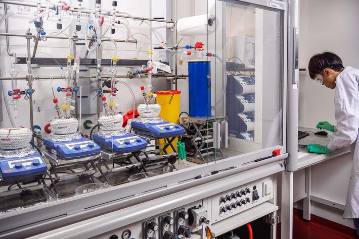
In her own research, Maria Ibáñez is investigating another area of application for nanoparticles: thermoelectrics. At the Werner Siemens Laboratory for Research on Thermoelectric Materials, she and her team are study-ing how electricity can be generated from a material’s temperature gradient using materials made of novel nanoparticles. While not new knowledge, the so-called thermoelectric effect is considered inefficient, especially as, with existing materials, only very little electricity is produced. That’s why a key part of Ibáñez’s project is accelerating the hunt for more suitable materials. To do so, her lab is constructing a high-throughput unit cap-able of simultaneously analysing and further developing hundreds of samples.
The high-throughput unit is extremely complex and will be made up of three parts, one each for synthesis, material preparation and measurement. For synthesis, the researchers select a powdery material they believe has promising thermoelectric properties. This results in dozens, or even hundreds, of variants that differ only in detail at the nanoscale, but that can present different properties.
In the material preparation section, the powders are converted into a type of ink and sprayed on foils that are subsequently exposed to a heat treatment and then examined—measured—in the unit’s third part. The measurement results are fed into a computer and analysed using machine learning. “Artificial intelligence helps us sift through the massive datasets and find the changes that are particularly interesting,” Maria Ibáñez says. At the moment, she and her team are focusing on material preparation. They’ve developed a prototype that will soon be ready for use. “Our high-throughput unit really began to take off last year,” Ibáñez says.
As a researcher, she’s fascinated by the search for more efficient materials and new, sustainable ways of using energy. But she also believes it’s important to not rely exclusively on technical advances—this, because the most effective tool for achieving energy sustainability is changing how we behave as consumers. “Finding a new technology that reduces energy consumption by twenty percent is very difficult. But saving the same amount would be easy to achieve if we adapted our behaviours.”
Recycling solvents
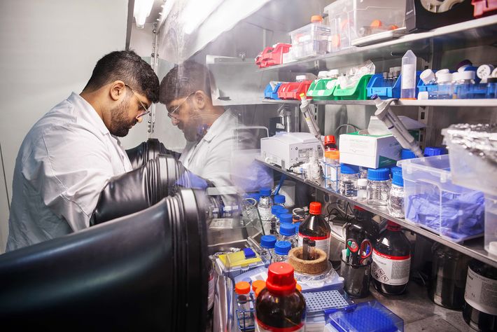
The principle of saving energy by changing consumer behaviour applies equally to the lab. In the past, Ibáñez says, experiments were run under optimal conditions only, no matter how much energy they consumed. “But today we try to see whether an experiment or a material will still work with less energy and waste.” Last year, her team focused on recycling solvents. “We fabricate our powders in special solvents and then separate them out,” she explains. “We used to throw the solutions away, but now we try to reuse them several times.” The team discovered they can use a solvent up to four or five times and still produce high-quality materials, which translates as up to seventy-five percent less waste.
Ibáñez says that exploiting the thermoelectric effect isn’t about saving huge amounts of energy all at once. But if less expensive, more efficient materials can make the technology competitive, it can still have a major impact. For instance, the thermoelectric effect could be used to supply electricity to smart sensors that, in future, will monitor temperature, lighting, air pressure and humidity in our homes or offices. Small electronic devices could also be charged using the technology. And, because the thermoelectric effect is reversible, it could also be channelled for cooling. “Transistors in electronic devices have to be cooled,” Ibáñez explains. Today’s cooling technology is based on ventilators. “But that doesn’t work well at the smallest level. Thermoelectrics could open up new horizons,” Ibáñez says.
Revolutionary single-atom switch
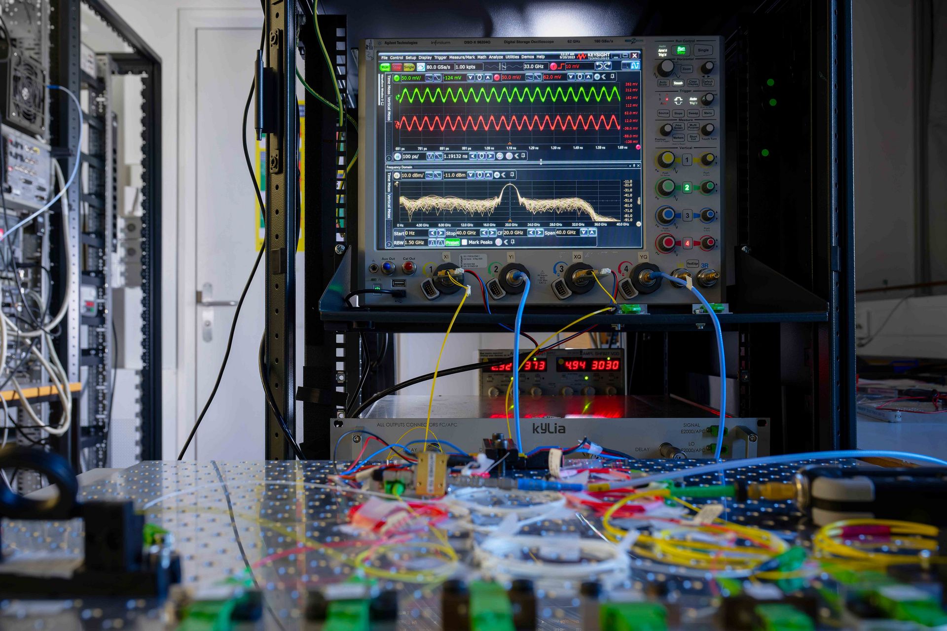
From espresso machines to huge mainframe computers, microchips are found in almost every electronic device we use. In recent years, researchers have succeeded in making microchips smaller and faster, but the push to get even more minuscule has now hit a wall, and the amount of energy the chips consume is a growing problem. That’s why researchers at the Center for Single Atom Electronics and Photonics at ETH Zurich and at the Karlsruhe Institute of Technology (KIT) are experimenting on a completely novel microchip—one that functions at the atomic level.
Funding from the Werner Siemens Foundation
12 million Swiss francs
Project duration
2017 to 2025
Project leader
Prof. Dr Jürg Leuthold,
head of the Institute of Electromagnetic Fields, ETH Zurich
Thrifty microchips
New horizons are also a keyword when it comes to the electronic components developed by Jürg Leuthold and his team at the Center for Single Atom Electronics and Photonics at ETH Zurich, which receives funding from the Werner Siemens Foundation. Leuthold is working on a completely novel type of microchip: one that switches on the basis of single atoms or ions rather than electrons, as is the current practice.
Energy consumption in digital devices in particular has spiked in the recent past; constant technical improvements and an unending supply of possible new functions are driving demand. New artificial intelligence programs are just one example, as Jürg Leuthold explains: “Technologies like ChatGPT work extremely well, but they start up their entire search engine to answer the simplest of questions. And that consumes an enormous amount of energy.”
The single-atom switch project could prove especially valuable in this regard. “We’re now working on next-generation microchips that could effectively boost energy efficiency by a factor of one hundred, even one thousand,” Leuthold says. This doesn’t mean we’ll consume a thousand times less energy for our communication needs, he adds, although studies have shown that, for the first time, global energy consumption for communication technologies has remained stable for about two years now, something that makes Leuthold optimistic. “This levelling out isn’t because demand is lower or fewer data were transmitted, but because technological innovation has brought about savings,” he explains. “New technologies are being developed that can do more with less energy.” In other words, the trend towards energy-saving devices and technologies is apparently able to offset our ever-growing hunger to communicate.
Leuthold’s group is at the forefront of this innovative research. Among their specialisations are so-called modulators—key elements in communication infrastructures that encode electrical signals onto laser beams. Indeed, modulators that convert electrical signals into optical signals are essential components in modern IT systems: information is stored electronically in our devices, our cell phones or in data centres, but the data are also distributed via fibre-optic networks in which photons (optical signals) function as information carriers.
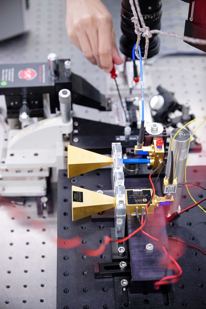
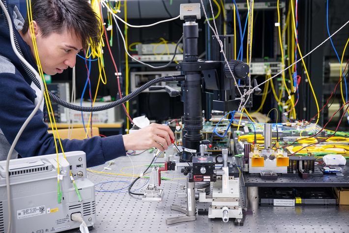
The researchers at ETH Zurich have now developed what are known as plasmonic phase modulators that enable extremely fast and efficient signal conversion. They’ve also demonstrated that these modulators can be used in various configurations for a wide range of applications, including the transition from a wireless LAN transmitter to an antenna in front of a house, as evidenced by a recently published study. “An amplifier mechanism is responsible for directly converting the signal,” Leuthold explains. “And the entire process needs one hundred to one thousand times less energy than a traditional modem.” PhD students in his group have now founded a start-up with the aim of commercialising these types of modulators.
Laser beams instead of deep-sea cables?
For a communication network to function properly, however, many other components besides modulators are needed. “There’s new momentum and innovation in many areas,” says Leuthold. As proof of this, researchers in his group have recently demonstrated how radically these innovations can change the world of communications technology. In a recent test carried out between the Jungfraujoch and the city of Bern, they demonstrated that optical data communication lasers are capable of transmitting data volumes of up to one terabyte per second through the air over long distances.
The experiment was a key step in showing that information can be transmitted via satellite through the atmosphere, even across great distances. “Already today, it’s easy to communicate in space using these lasers,” Leuthold says. But because air turbulence in the atmosphere interferes with transmission, he and his European partners combined various innovations to ensure that large datasets are still readable, despite the disruption. If the technology makes the leap to application, it will replace the incredibly expensive deep-sea cables that currently form the backbone of the global internet.
Superfast switches
In addition to these advances, there’s always the chance that Leuthold’s group will land yet another coup with the WSS single-atom switch project. And they’re certainly well on the way: the researchers have already demonstrated that the new method significantly boosts energy efficiency, and last year they published a study proving that the novel single-atom switch can also compete with traditional switches in terms of speed. A veritable breakthrough.
Speed is critical. Even if the switches are as small as technically possible, if they react sluggishly when turned on and off, they’ll never find practical application. Leuthold and his team managed to lower the switching time to less than twenty picoseconds—a picosecond being a millionth of a millionth of a second, which is more or less what today’s silicon chips achieve. This means that switching speed will no longer be a reason to rule out single-atom switches.
The team scored yet another breakthrough last year in the area of switching types. In electronics, a basic distinction is made between volatile and non-volatile switches: volatile switches return to the starting position after activation, while non-volatile switches remain active until their status is changed. For the first time, Leuthold’s team has succeeded in constructing both types using their single-atom switch method. “This is very important, as it enables us to expand our toolkit,” Leuthold explains.
For the next few years, the researchers will be concentrating on connecting the various elements. “Up to now, we’ve been focusing on the single switch,” Leuthold says. “But at the end of the day, we need to link several switching elements together if we’re to realise a function.” It’s a function that promises to be a clever way to at least keep energy consumption in check.

Revolutionary single-atom switch
From espresso machines to huge mainframe computers, microchips are found in almost every electronic device we use. In recent years, researchers have succeeded in making microchips smaller and faster, but the push to get even more minuscule has now hit a wall, and the amount of energy the chips consume is a growing problem. That’s why researchers at the Center for Single Atom Electronics and Photonics at ETH Zurich and at the Karlsruhe Institute of Technology (KIT) are experimenting on a completely novel microchip—one that functions at the atomic level.
Funding from the Werner Siemens Foundation
12 million Swiss francs
Project duration
2017 to 2025
Project leader
Prof. Dr Jürg Leuthold,
head of the Institute of Electromagnetic Fields, ETH Zurich